(Click on any of the images below to enlarge them.)

The Niskayuna facility is the largest of several GRCs. GE also has centers in Munich, Germany; Bangalore, India; Shanghai, China; Rio de Janeiro, Brazil and San Ramon, California.
The history of invention and innovation that has taken place at GRC to create major new businesses was on display as we walked along the entry hall. Some highlighted examples include x-ray medical imaging, jet engines, magnetic resonance imagers, digital x-ray panels and a number of other world firsts. The Research Center in Niskayuna is one of the world's largest corporate R&D centers that conducts focused, strategic research and development. This is GE -- after all -- and GE has the demonstrated ability to identify new business opportunities, utilize its research capacity to develop the required technologies in collaboration with GE businesses, and then to grow these businesses globally. As such, the master plan needs significant R&D capability to back it up.
The GRC R&D programs are divided between longer term projects (Advanced Technology programs) and projects that develop technology for one or more GE products in a two to five year time frame. GE business divisions (i.e. GE Aviation, Healthcare, Energy, Oil and Gas, etc.) fund the shorter term, targeted R&D projects and researchers at the Center therefore have an internal business customer. GRC is responsible for meeting the needs of that business, and the businesses frequently visit the Center to review technical progress.
GRC has been conducting research in MEMS since 2002. The objective of this research is to create new MEMS components that are not commercially available and that enable a breakthrough feature or strengthen the value proposition of a GE product. One of the most impressive MEMS devices that I learned about at GRC is a MEMS microswitch -- GRC researchers claim this switch to be the fastest switch that acts as a mechanical relay (vs. solid state, semiconductor switches). Through applied and focused R&D, the brilliant scientists at GRC have created a MEMS microswitch that handles over a kilowatt of power (240 Volts AC and 7 Amps). For its industrial applications (just for starters) this MEMS microswitch reduces the time required to interrupt a fault current (short circuit) from milliseconds (the switching speed of conventional circuit breakers) to a few microseconds (for a breaker made from MEMS switches).
It is equally amazing that these researchers were able to utilize a novel set of materials to construct the MEMS switches (GRC's "secret sauce"). The switch materials and the process flow are compatible with both silicon and quartz substrates, and it may be possible to fabricate these switches on completed CMOS wafers. The novel materials play a key role in enabling the fabrication of the robust, reliable and mega-power-conveying MEMS microswitches. In addition, GRC also does all the failure mode analysis, reliability testing, and most of the packaging for the microswitches; as well as most of the other MEMS they R&D and fab onsite. It's quite an impressive operation.
Chris Keimel of GRC presented an abstract on the MEMS microswitch at Hilton Head Workshops in June 2012. His paper created a lot of buzz; and as more folks learn about it I am confident that the buzz will turn into a loud roar of applause (maybe this blog will help; I can only humbly hope so!).
Beyond the research being done at universities and research institutes in the US and abroad, I can think of only one other example (in the MEMS field) of a company doing this level of sophisticated commercialization-focused research; Robert Bosch GmbH (and they are privately-held; GE is not).
But what makes GRC unique is that for MEMS, not only do these guys do the R&D at GRC, they also do the pilot volume fabrication. With their new expanded cleanroom facility (nearly 30,000 sq. ft.); they are doing amazingly cool stuff in MEMS. From what I learned on the full head-to-toe bunny suit tour that I had with fab manager, Ron Olson, GRC is fabricating both silicon carbide based power MOSFETs and MEMS for GE at an impressive rate. By no means is this a high-volume fab; but these guys have a sophisticated operation that is able to accommodate both the R&D and the pilot volume needs of GE's businesses in a single facility.
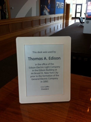
Lastly, no visit to the facility can be complete without a mention of the beauty of the place. It truly is gorgeous, especially in July (maybe a bit cold in January?). The rate of turnover at GRC is low and I can see why; why would you want to leave this place? You get to work with brilliant scientists, doing great commercially focused R&D, actually manufacture products and live in a beautiful part of the country. As Thomas Edison once stated: "I never perfected an invention that I did not think about in terms of the service it might give to others." Clearly at GRC Niskayuna, his legacy lives on.
No comments:
Post a Comment